Output Submodule
The output submodule of the GPU generates a valid VGA signal using the signals from the counter module and reads data from the memory module.
Address building
Depending on the current mode, there are two ways to construct the address from the counter values.
This is done through hard-wiring both combinations to MUX chips (including the static part in the beginning of the text mode address) and selecting the one we want based on the cached mode select bit.
Mode switching
To be able to achieve mode switching we need two things:
- Clear the mode after one line is done
- Set the new mode before the next line begins
The mode is cleared as soon as hsync becomes low. This signal resets the 74HCT74-flipflop to switch to text mode. On the delayed rising edge of hsync (the end of hsync) the lowest bit of the 94th byte in the current line is loaded to set the mode. By that time the y counter has already been incremented, so that we can set the bit in the same line (not the line before to avoid additional logic for the first line in the software).
Resetting to text mode is easier since we read the same bit for the entire text line (and not two different ones as it would be the case for the image mode).
VGA signals
To produce a working VGA signal, we need the following data signals (pin on the VGA connector):
- RED (1)
- GREEN (2)
- BLUE (3)
- HSync (13)
- VSync (14)
hsync and vsync are taken directly from the counter module. The color channels are analog, so we need to convert each of the 2bit digital signals. This is achieved using a resistor ladder making use of the standardized 75 ohm resistance of cable and monitor. The values for the resistors have been calculated by Ben Eater for his graphics card.
Data pipeline
To be able to decode the characters we need a data pipeline since the flash chip for the character ROM and the memory are not fast enough to do everything in one step. We are always handling both text mode decoding and image mode at the same time and select the wanted result afterwards.
Text mode
When the data from memory is stable, it is stored in the first register to guarantee that the character ROM gets a stable signal. The character ROM decodes the character using the 4 lowest bits of the y-counter (character is 16 pixels high) and the byte representing the character. This results in 8 bits representing whether the next 8 pixels are black or white.
The next step is the shift register: it loads the character every 3.125 MHz using an edge detector on the corresponding clock signal and shifts out one bit at a frequency of 25 MHz. This enables us to use the full resolution of 640x480. To get a 2 bit color we simply use the output of the shift register as both low and high value for all color channels resulting in black or white output.
The clock division is done by using the lower bits of the x counter since we only divide the clock by a power of two. The base frequency is 25 MHz, so we use a division by 4 (6.25 MHz) for every pixel and by 8 (3.125 MHz) for every character.
Image mode
The image mode pipeline just delays the signal to match the data of the image mode. It uses the first register and the pixel register.
Schematics
Chip Layout
In the Build
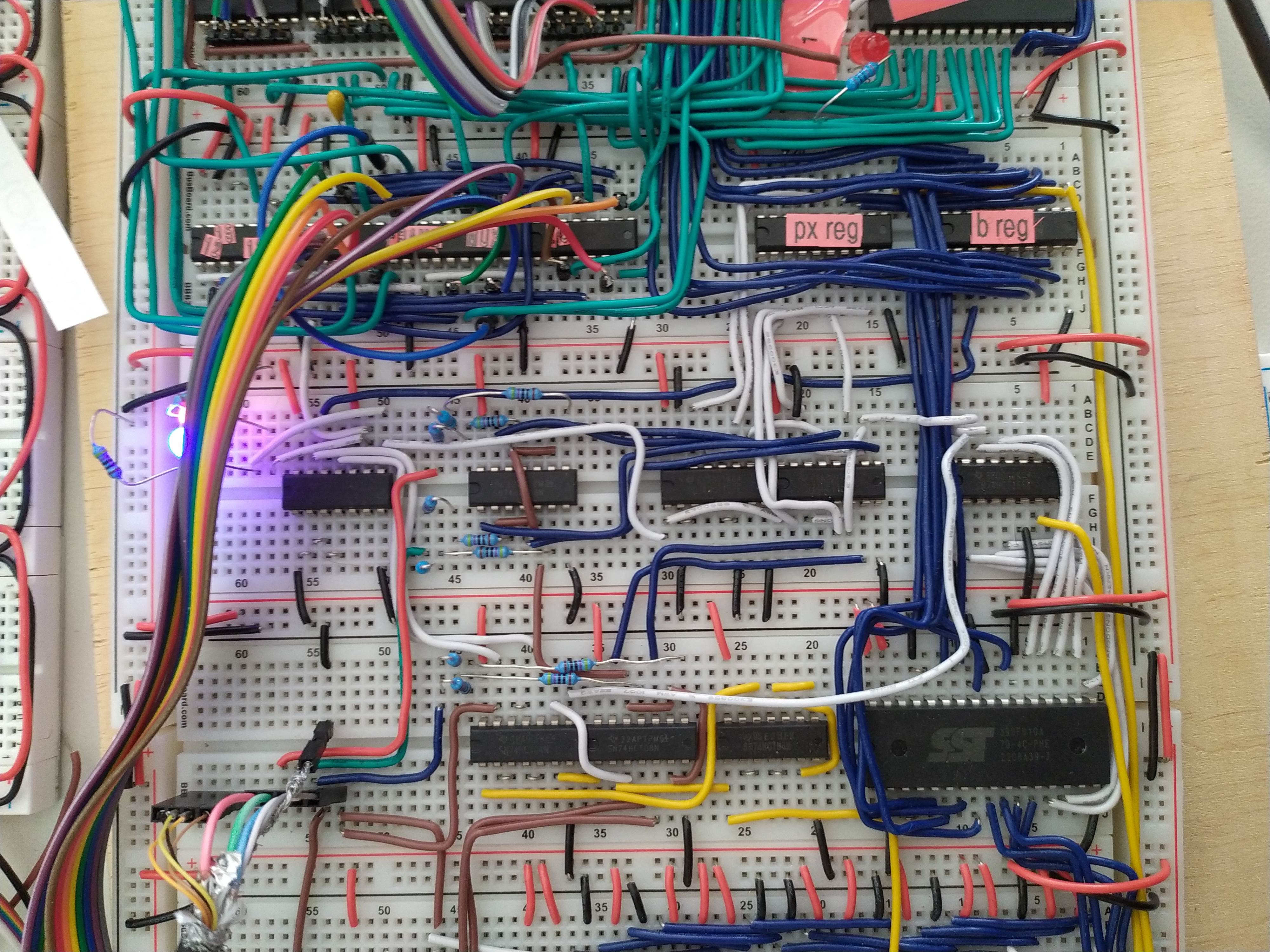
The first register is labeled as b reg in this picture.


