Memory Submodule
This part of the GPU essentially handles the routing between two address buses, two data buses, and two RAM chips.
The general idea is that the CPU address and data bus are connected to one RAM chip, while the GPU is connected to the other. While FB_SEL is high, the two are switched.
Schematics
Chip Layout
Addresses
Since the address buses are one-directional, multiplexers are used to switch which address bus is currently connected to which RAM chip. Since we use an 16-bit address bus, this means that 4 quad-2-to-1 multiplexers are used for each framebuffer.
Data
Two different solutions are used for the data buses to reduce complexity.
- For the data going from the graphics RAM to the graphics card output, since it is one-directional, multiplexers are again used to select the output of the proper graphics RAM chip.
- For the CPU data bus, bus transceivers are used.
Control Line Logic
Since the CPU treats the graphics card as if it was a single framebuffer (same addresses for both chips), control lines need to be combined in various ways to only write to the proper chip.
For one, the GPU uses only the upper half of the I/O memory region (the lower half can be used for other devices), therefore, any signals should only have an effect if both ADDR16 (the additional 17th address line) and the highest address bit are 1.
Then, both BUSREQ and IO/MEM_TO_DBUS are combined with this signal and FB_SEL (or ~FB_SEL) to generate distinct signals for each RAM chip.
Of these, the IO/MEM_TO_DBUS signal controls the direction of the bus transceiver, while BUSREQ enables it.
Finally, IO/MEM_TO_DBUS on the RAM chips must only be active while the data is stable. Therefore, this signal must be a combination of IO/MEM_TO_DBUS and BUSREQ for the relevant chips.
The enable signal going to the bus transceiver is OR-ed with itself in order to introduce the same delay here, so that the transceiver does not stop outputting before the RAM stops writing.
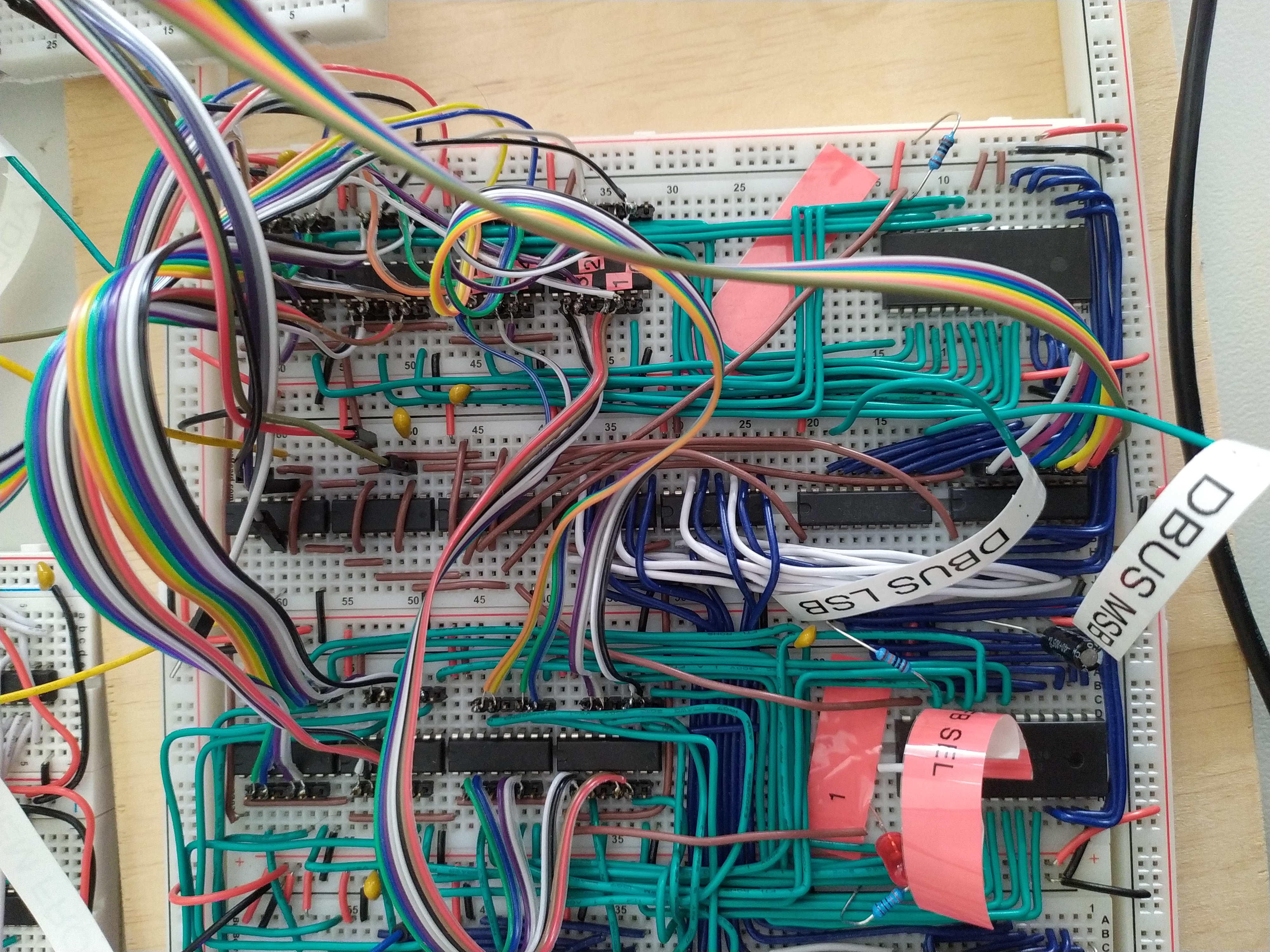
In the Build


